


Please Leave Us A Message
Privacy statement: Your privacy is very important to Us. Our company promises not to disclose your personal information to any external company with out your explicit permission.

Yetnorson
 December 28, 2022
Since the modern era, mobile communication technology has developed rapidly and is becoming more and more popular. Wi-fi technology is an important part of modern wireless communication technology. Due to its low profile, good directionality, high fabrication feasibility, low cost, conformability to the surface of the object, and easy array formation, the microstrip antenna has been widely favored; therefore, Wi-fi technology and microstrip antennas Technology is a hot topic in recent years.
ANSYS HFSS software is a three-dimensional electromagnetic field simulation software based on adaptive meshing technology introduced by ANSYS. It is the main design and analysis tool for high-frequency design, and it is playing an increasingly important role in the development of RF products. Designing antennas using HFSS software can automatically obtain various antenna parameters such as gain, directionality, far field pattern profile, and far field 3D map. With ANSYS HFSS you can calculate:
1) Divide the structure into a finite element mesh (adaptive meshing);
2) Calculate the mode supported by the transmission line having the same cross section as the port at each excitation port;
3) Assuming that each mode is excited, all electromagnetic field modes within the structure are calculated;
4) Calculate the generalized S matrix from the obtained amount of reflection and the amount of transmission.
A variety of active and passive devices can be designed in conjunction with other ANSYS series simulation software such as Ansoft Designer. ANSYS HFSS is currently the mainstream software for microwave engineering design. How to better learn and use ANSYS HFSS software technology, so as to give full play to the efficiency of software, reduce the labor level of engineering design, improve engineering design efficiency is the main problem we have to solve.
1. Calculation and analysis of the antenna model1.1, the design of the antenna radiation element
The transmission line mode method is used to analyze the radiation principle of the microstrip antenna. The length of the radiating element is L, the width is W, and the thickness of the dielectric substrate is h. The radiating element, the dielectric substrate and the grounding plate are regarded as a length L. The microstrip transmission line is broken at both ends of the transmission line to form an open circuit. Due to the thickness h of the substrate, "λ, the field is evenly distributed along the h direction, there is no change in the width W direction, but only in the length L direction, in two At the open end, the electric field can be decomposed into a vertical component and a horizontal component. The two vertical components are opposite in direction and thus canceled in phase, and the far-field fields generated by the component directions generated by the two horizontal components are identical and superimposed in phase. The radiation of the microstrip antenna can be equivalent to a binary array consisting of two slits. The width W is approximated by the following formula

The model of a single radiating element and the electric field distribution on the radiating element are calculated by calculation and ANSYS HFSS software simulation as shown in Figure 1-1.
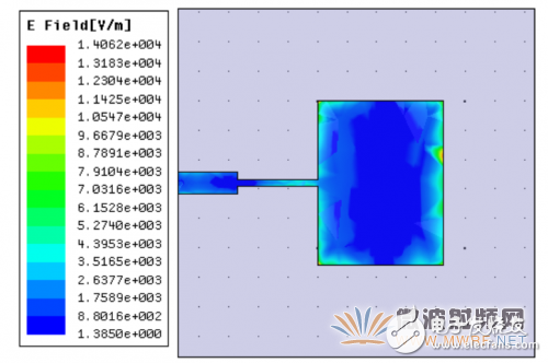
Figure 1-1 Model and electric field distribution of a single radiating element
1.2, matching network design
In this case, a 3dB aliquot splitter is required to connect the two radiating elements and the external stimulus. The power splitter is a three-port network, as shown in Figure 1-2. The input resistance is Z1, and the resistances of the two outputs are Z2 and Z3. Because the bisector splitter structure is symmetrical, Z2 and Z3 Equal, in order to make no reflection between port 1 and port 2, 3, according to the principle of transmission line, should be

In order not to reflect, Zin1∥Zin2=Z1. Different impedances corresponding to different line widths in the microstrip line are used to establish a three-dimensional model on ANSYS HFSS according to the above conversion relationship. The calculation of the three-port scattering parameters by ANSYS HFSS determines the shape of the power divider.
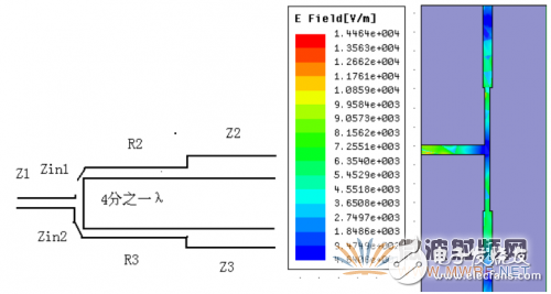
Figure 1-2 Schematic diagram of the power splitter Figure 1-3 Modeling of the power splitter based on ANSYS HFSS
1.3, the overall design of the antenna
With the design of the radiating element and the matching network, the whole is the combination of the two, combined with the actual requirements, through the use of ANSYS HFSS software for a series of simulation optimization, and finally selected the structure of the double-layer microstrip array.
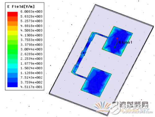
Figure 1-4 Optimized antenna model and radiation element electric field distribution
2. Analysis of optimization results of antenna modelIn the antenna design index, the radiation direction, the working bandwidth, the radiation gain, the voltage standing wave ratio VSWR, and the traveling wave reflection coefficient S11 of the input port are several important aspects that must be considered. The ANSYS HFSS software is based on adaptive meshing technology. Users can easily set the material type, boundary conditions and physical dimensions to solve the full-wave analysis of any 3D model. The ANSYS HFSS software calculates the main antenna design parameters.
2.1. Analysis of antenna gain parameters
The radiation direction and gain of the antenna can characterize the bundling ability of the radiated energy of the antenna and the efficiency of the input power obtained by the antenna from the transmission line into the radiated power, which is not only related to the direction range and distance range of the electromagnetic wave transmission, but also related to the transmitting capability and reception of the antenna. Sensitivity. Factors affecting the gain of the day in the microstrip antenna include the following aspects
1 the loss of the dielectric substrate;
2 surface wave loss radiated by the antenna;
3 directional strength;
4 Match the matching between the network and the input;
5 conductor loss of the antenna structure.
Figure 1-1 shows a structure of a single radiating element, the material of which is Rogers TMM (4), the relative dielectric constant is 4.5, and the loss tangent is 0.002. The structure shown in Figure 1-4 is a binary antenna array. There are two differences in the structure. First, the array is used to enhance the directivity and increase the gain in the direction of the emission. Second, the air dielectric layer is added, and the loss tangent of the air is almost zero, which reduces the loss of the antenna and increases the gain. The above two points are verified by the comparison of Figure 2-1 and Figure 2-2.
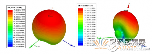
Figure 2-1 Single-layer unary antenna gain map Figure 2-2 Double-layer array antenna gain map
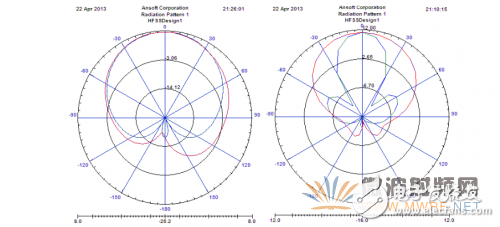
Figure 2-3 Two-dimensional orientation of a single-layer unary antenna Figure 2-4 Two-dimensional orientation of a two-layer array antenna
As shown in Figure 2-1 and Figure 2-3, the single-layer unary antenna has a horizontal lobe width of 100 degrees, a vertical lobe width of 95 degrees, and a gain of 7.5 dB. As shown in Figure 2-2 and Figure 2-4, the two-layer array antenna has a horizontal lobe width of 90 degrees, a vertical lobe width of 35 degrees, and a gain of 11.2 dB. The effect of optimization is still quite significant.
2.2. Analysis of antenna reflection parameters
In microwave circuits, voltage and current cannot describe the characteristics of the circuit due to high frequency characteristics and are difficult to measure. In order to characterize the characteristics of a microwave circuit, it is necessary to use scattering parameters that can be directly measured at microwave frequencies. Also referred to as the S parameter, specifically to the field of antennas, since only the input port needs to be studied, only one type of scattering parameter is needed, which is the S11 parameter, which represents the ratio of reflection and incidence of the input port. In the ordinary sense, the S11 and the voltage standing wave ratio VSWR can be mutually converted, that is to say, sometimes the S11 and the voltage standing wave ratio VSWR need only observe one kind, and this paper chooses to observe S11. In general, S11 can not only express the utilization of input power, but also observe the operating bandwidth of the component according to S11 at different frequencies. The smaller the power utilization of S11, the higher the S11 is below -15dB.
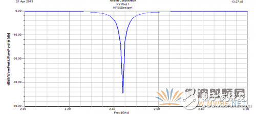
Figure 2-5 Single-layer unary antenna S11 parameters
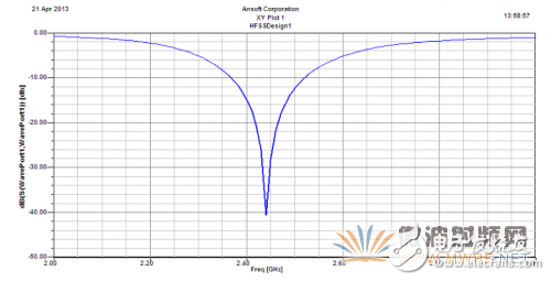
Figure 2-6 Double-layer array antenna S11 parameters
The microstrip antenna in this example is a resonant antenna, and generally only works near the resonant frequency, and the frequency band is relatively narrow. For practical needs, research on broadening the bandwidth of microstrip antennas is a development direction today. In general, the thickness and dielectric constant of the dielectric plate are the main factors affecting the operating bandwidth of the microstrip antenna. In this paper, by increasing the thickness of the medium by increasing the use of the air dielectric layer, the effect of widening the working bandwidth is achieved.
The above is the Detailed process of design and optimization of WiFi antenna based on ANSYS HFSS software we have listed for you. You can submit the following form to obtain more industry information we provide for you.
You can visit our website or contact us, and we will provide the latest consultation and solutions
Send Inquiry
Most Popular
lastest New
Send Inquiry
Privacy statement: Your privacy is very important to Us. Our company promises not to disclose your personal information to any external company with out your explicit permission.
Fill in more information so that we can get in touch with you faster
Privacy statement: Your privacy is very important to Us. Our company promises not to disclose your personal information to any external company with out your explicit permission.